
60–90% of PCB assembly failures stem from solder paste-related issues, not component orientation.
Solder defects frequently escape end-of-line inspection and reach field deployment.
Solder joint failures occur when components experience thermal stress combined with power loads exceeding manufacturing tolerances.
Real-time measurements of solder volume can predict fatigue lifetime and improve discretion on acceptable vs. rejected boards.
Real-time solder volume measurement enables predictive fatigue analysis, improving accuracy in board acceptance and rejection decisions.
Statistical process control on paste printing represents a critical quality gate for achieving sub-50 DPMO performance.
Data collection and analytics are becoming essential for improving quality and ensuring reliability, particularly in safety-critical applications where (data sharing across equipment) enhances defect detection and root cause analysis.
Thermal and Environmental Stress Factors
Temperature fluctuations in production facilities (optimal range: 20–25°C) directly impact soldering quality and introduce corrosion defects.
Humidity levels outside 40–60% range compromise solder joint integrity during assembly.
In-field thermal stress combined with electrical loads causes solder joint failures that initially pass manufacturing inspection.
Cabinet environments in deployed IoT devices can reach temperatures sufficient to degrade marginal solder connections.
Repetitive mechanical stress in flexible PCB applications causes copper trace cracking and connection failures after extended use.
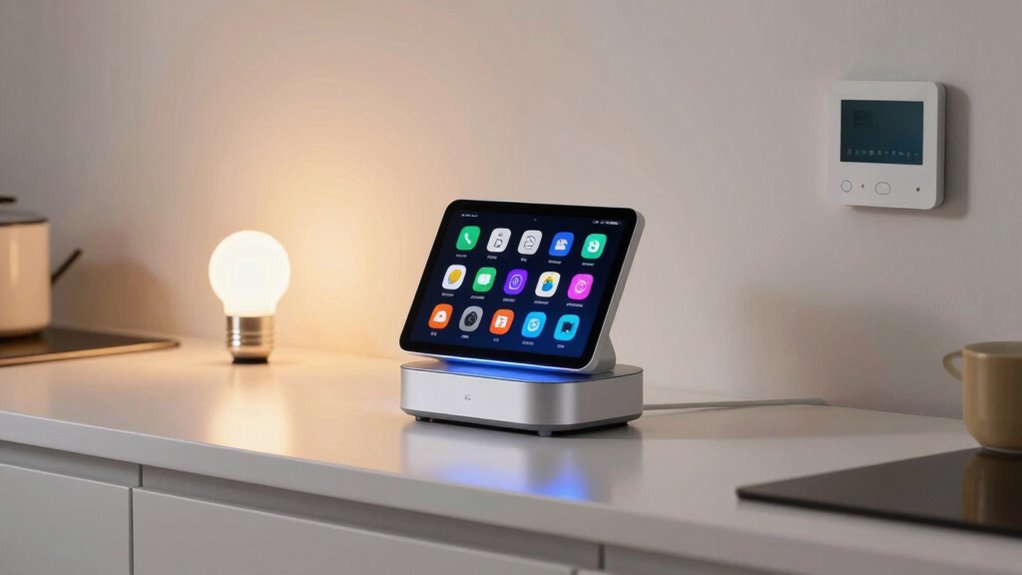
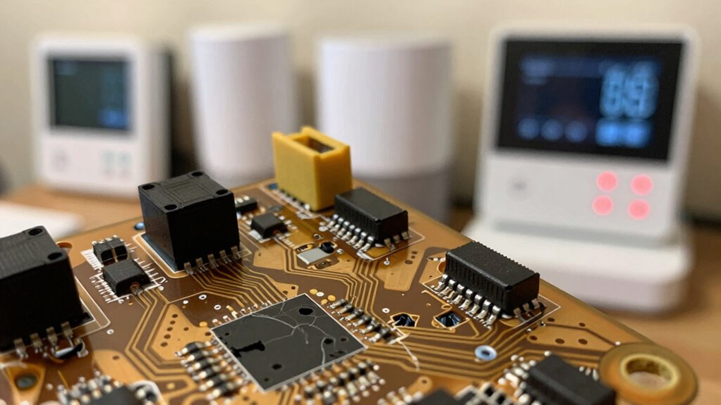
Smart speakers like Echo devices require especially robust PCB assembly as they operate continuously while processing voice commands through the Alexa software.
Component Misalignment and Mechanical Failure
Component misalignment accounts for approximately 20% of PCB assembly failures within the broader defect category.
Misalignment of 0.1mm in high-speed production can lead to connectivity issues and open circuits.
Mechanical enclosure processes during box build can cause physical changes impacting electrical performance.
Antenna array positioning changes (minor displacement of “princess arrays”) can severely degrade wireless functionality.
Missing parts and wrong component placement comprise approximately 15% of assembly-related failures.
Testing and Inspection Gaps
In-circuit testers (ICTs) fail to log parametric test data due to test time bottlenecks in high-volume production.
PCB end-of-line (EOL) testers exhibit wide variations in measurement accuracy, leading to increased scrap and poor quality shipments.
Board electrical testing limited to simple connectivity checks (opens/shorts) misses performance variation insights.
Lack of RF/WiFi system-level testing allows wireless performance degradation to escape to customers.
Recommended testing combination includes flying probe tests, automated optical inspection (AOI), and manual functional verification by design engineers.
Parametric Measurement and Predictive Analytics
Advanced sensor data capturing parametric measurements (frequency, voltage, current, capacitance, resistance, settling times) enables reliability predictions.
Solder volume measurements via real-time sensors can predict fatigue lifetime before field failures occur.
Aggregation of defect data from millions of units reveals solder defects as number 4 in top 10 failure cause.
World-class assembly performance is achievable when partners consistently meet sub-50 DPMO benchmarks, ensuring higher reliability in wireless sensor deployments.
References
- https://semiengineering.com/demand-grows-for-reducing-pcb-defects/
- https://camptechii.com/pcb-assembly-failures-dfm-guidelines-yield-reliability/
- https://pmc.ncbi.nlm.nih.gov/articles/PMC8656411/
- https://www.allpcb.com/blog/pcb-manufacturing/the-hidden-costs-of-pcb-defects-mastering-quality-control-in-mass-production.html
- https://www.elecrow.com/blog/top-10-testing-methods-for-high-quality-pcb-assembly.html
- https://www.allpcb.com/allelectrohub/the-hidden-costs-of-poor-pcb-quality-a-financial-impact-analysis
- https://www.ednasia.com/how-5g-wireless-is-impacting-the-pcb-design-and-manufacturing/
- https://www.agicent.com/blog/cb-assembly-in-iot-app-development/
- https://www.wonderfulpcb.com/blog/pcb-manufacturing-assembly-smart-home-electronics-requirements/